
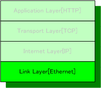
Internet Protocol Suite
The hardware part of the Link Layer is constructed with CPU, FPGA including Ethernet MAC Core, PHY chip , pulse trans chip, etc.
System Architecture
The following shows system architecture and building blocks in the FPGA.
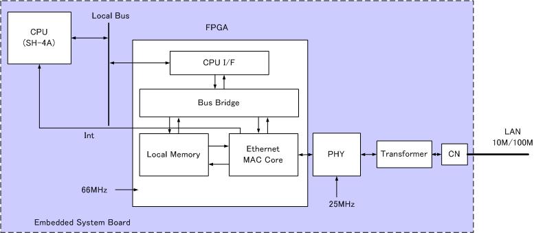
System Architecture
- CPU is SH-4A
- Ethernet MAC Core is implemented in the FPGA(Spartan3 XC3S400).
- Ethernet MAC Core uses Block RAM in the FPGA as Local Memory.
- PHY Chip(LAN83C185) is connected to the FPGA using MII.
- PHY is connected to RJ45 connector via Pulse Trans(TLA-6T118)
- 66MHz for FPGA core clock( CPU local bus clock)
- 25MHz for PHY
- An Interrupt signal is used for communication between CPU and Ethernet MAC Core(IR21)
Building Blocks in FPGA
FPGA top module is constructed with four modules including Ethernet MAC Core.
| Module Name | Description |
|---|---|
| CPU I/F | CPU(SH-4A) Bus Interface |
| Bus Bridge | Bridge interface between CPU Bus and WHISHBONE*1 |
| Ethernet MAC Core | OpenCores Ethernet IP core |
| Local Memory | Local buffer to store Ethernet Frame |
CPU I/F module is an interface module for SH-4A Local Bus. Local Bus protocol is configured to SRAM type, mapped on CS2 space, and accepts single read/write transfer. Bus Bridge module converts interface protocols between CPU and WISHBONE. Local Memory is an SRAM memory implemented by FPGA Block RAM and stores Ethernet Frame. Ethernet MAC Core transmits and receives Ethernet Frame. The Core transmits Frame data from Local Memory to PHY, and receives Frame data from PHY and send it to Local memory.
Memory Mapping
The FPGA is mapped in Sh4 area2 memory space. The internal resources in FPGA are mapped on 16MByte boundary in area2 by each function. Ethernet MAC Core registers are mapped to address space 0x0A00_0000-0x0A00_07FF、4K Byte Local Memory is mapped to address space 0x0A80_0000-0x0A80_0FFF.
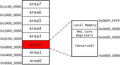
SH4 Memory Mapping
RTL Simulation
Basic behavior of Ethernet Frame transfer is confirmed in RTL simulation. The functional simulation environment contains FPGA top module, PHY model, and CPU Bus Function Model(BFM). BFM is written in verilog task and handles CPU local bus read/write transaction.
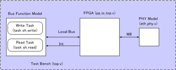
Simulation Environment
The following test bench initializes PHY and Ethernet MAC core, then transmits and receives Ethernet Frames.
(top.v, a part of the test bench)
 /***********************************************
     Main test routine
 ***********************************************/

 initial begin
     reset;
     phy_setup;
     register_setup;
     set_tx_frame;
     send_tx_frame;
     set_rx_frame;
     receive_rx_frame;
     repeat (1000) @(posedge L_CLK); // inter packet gap
     receive_rx_frame;
     repeat (100) @(posedge L_CLK);
     $finish;
 end
Logic Synthesis
The following shows FPGA resource usage, synthesized with xst in ISE.
| Logic Utilization | |
|---|---|
| Number of Slice Flip Flops | 1,232 out of 7,168 17% |
| Number of 4 input LUTs | 2,417 out of 7,168 33% |
| Logic Distribution | |
| Number of occupied Slices | 1,618 out of 3,584 45% |
| Number of RAMB16s | 6 out of 16 37% |
*1 An interconnect architecture which is recommended in OpenCores project.